Explore Maine by Region
Browse popular destinations by region, discover must-do experiences, as well as the best places to stay and eat.
Click on the map to start exploring.
Highlands
The highlands area is home to not only Maine's highest peak on Mount Katahdin, but also to the state's largest lake, Moosehead Lake. This region is an absolute must for the outdoorsman, offering more than 200 waterfalls, exceptional snowmobiling opportunities throughout the winter months and endless wildlife sightings during warmer weather. In fact, it's said to be the best place in the state of Maine to spot a moose!
Aroostook County
If you’re looking for outdoor adventures in the northernmost part of the state, Aroostook County is the place to visit. Aroostook County is commonly referred to as “The Crown of Maine,” not only because of it's location within the state, but also because of the exceptional views, wildlife, charming towns and friendly people. This region borders the Canadian provinces of Quebec and New Brunswick.
Downeast & Acadia
Downeast Maine embodies the state’s incredible coastal spirit. From Acadia National Park, to the town of Bar Harbor, this region is filled with spectacular views and tons of activities for visitors to take advantage of. The towns of Machias, Calais, Eastport make up this region, along with Mount Desert Island (MDI) which is the largest island off the coast of Maine. The Downeast area attracts thousands of nature lovers, bird watchers and hikers to the state throughout the spring and summer months. Charter a boat for deep sea fishing, or join a whale watching excursion for a fun day on the ocean. If you’re visiting during the snowier months, common winter activities include enjoying the local French cuisine and visiting the local shops throughout Bar Harbor and its neighboring towns.
Mid-Coast Islands
Located on the gorgeous coastline of Maine, the Mid-Coast Islands are ideal for whale watching, grabbing the best seafood in the country or simply exploring small town Maine. The picturesque towns of Wiscasset, Camden, Rockland, Belfast, Brunswick, Damariscotta and others are located in this region, offering stunning year-round coastal views for residents and tourists alike.
Kennebec Valley
Stretching 170 miles, the Kennebec Valley sits in the center of Maine. This area includes not only one of Maine's most prestigious colleges, Colby College in Waterville, but also the former mill town of Skowhegan and the state capitol of Augusta. In the Kennebec Valley, visitors can enjoy everything from exploring the artsy town of Hallowell, to white water rafting in the Forks.
Lakes & Mountains
The lakes and mountains region of Maine is home to the scenic towns of Rangeley, Fryeburg, Lewiston and Auburn, Farmington, Bethel, Naples and many others. Whether you're looking to enjoy a pristine day fishing Rangeley Lake or hiking the mineral and gemstone quarries within the Oxford Hills Region, this part of the state is one you won't want to miss. Discover some of the best places for white water rafting, charming small towns, and much more here.
Greater Portland
Maine’s southern region offers a diverse range of fun. From the bustling streets of the state’s biggest city, Portland, to the more tranquil feel of smaller towns such as York, Ogunquit, and Kennebunk. If you’re looking for incredible restaurants and the opportunity to shop, Portland’s Old Port is packed with local boutiques and trendy places to grab a bite. Just 25 minutes north of Portland is Freeport, home to L.L Bean and lots of other outdoor outlet stores. Ultimately, southern Maine is known best for its historic architecture, breathtaking beaches, quaint coastal towns and beautiful lighthouses. Don’t miss the opportunity to shop, dine and explore this memorable region.
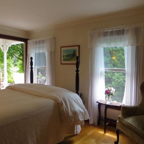
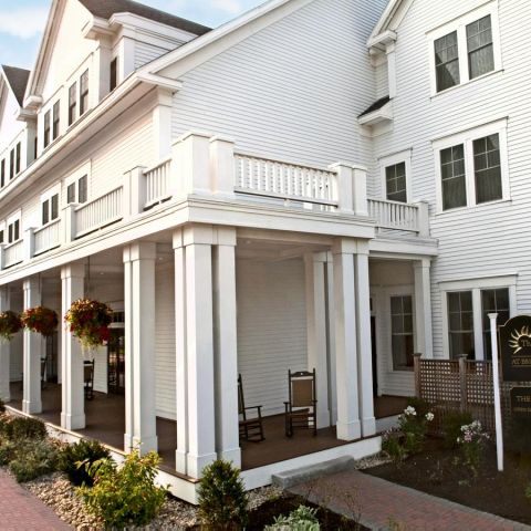
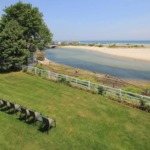
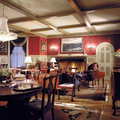
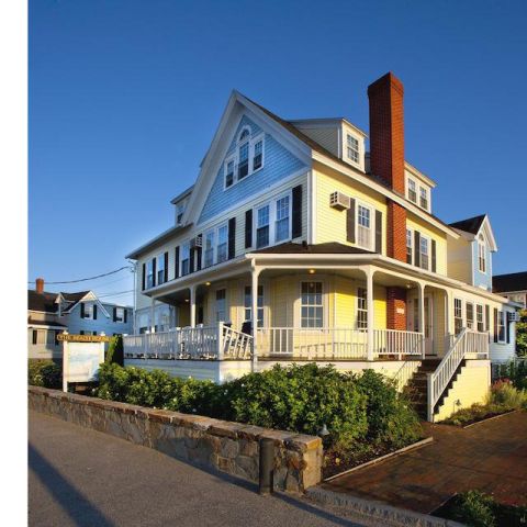
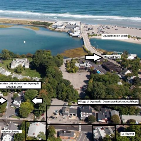
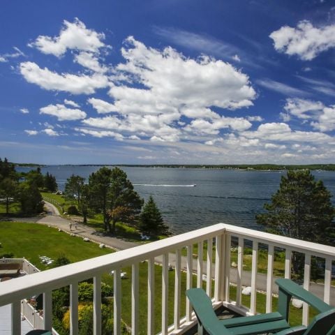
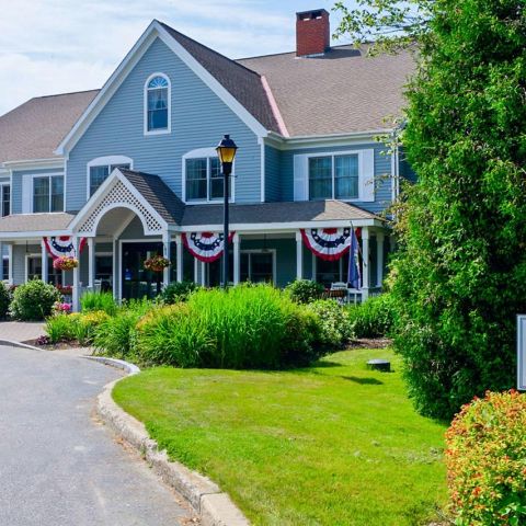
Southern Maine Coast
Maine’s southern region offers a diverse range of fun. From the bustling streets of the state’s biggest city, Portland, to the more tranquil feel of smaller towns such as York, Ogunquit, and Kennebunk. If you’re looking for incredible restaurants and the opportunity to shop, Portland’s Old Port is packed with local boutiques and trendy places to grab a bite. Just 25 minutes north of Portland is Freeport, home to L.L Bean and lots of other outdoor outlet stores. Ultimately, southern Maine is known best for its historic architecture, breathtaking beaches, quaint coastal towns and beautiful lighthouses. Don’t miss the opportunity to shop, dine and explore this memorable region.